E-ISSN:2583-553X

Research Article

Photoluminescence

Applied Science and Biotechnology Journal for Advanced Research

2025 Volume 4 Number 3 May
Publisherwww.vandanapublications.com

Tuning Optical and Electronic Properties of MoS₂ and MoSe₂ Crystals via External Pressure: Structural Analysis and Device Implications

Mor B1*, Korot K2
DOI:10.5281/zenodo.15795690

1* Bhupendra Mor, Lecturer, Department of Physics, Science & Humanities, Government Polytechnic, Palanpur, Gujarat, India.

2 Kirti Korot, Assistant Professor, Department of Physics, Science & Humanities, Government Engineering College, Palanpur, Gujarat, India.

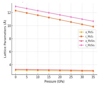
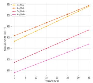
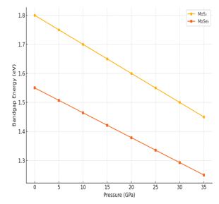
Layered transition metal dichalcogenides (TMDs), particularly molybdenum disulfide (MoS₂) and molybdenum diselenide (MoSe₂), have garnered substantial attention due to their tunable bandgaps, strong excitonic effects, and layered structures. These unique properties render those promising candidates for next-generation optoelectronic and nanoelectronic devices. In this study, we investigate the structural and optoelectronic modulation of high-purity single crystalline MoS₂ and MoSe₂ under externally applied pressure up to 35 GPa using a diamond anvil cell (DAC) setup. Through in-situ synchrotron X-ray diffraction (XRD), Raman spectroscopy, and photoluminescence (PL) measurements, we observe pressure-induced lattice compression, phonon mode shifts, exciton quenching, and bandgap narrowing, without any evidence of structural phase transition up to the studied pressure range. These findings offer insight into pressure-driven band structure engineering and highlight the potential of TMDs for pressure-tunable optoelectronic devices.

Keywords: MoS₂, MoSe₂, high pressure, optoelectronics, raman spectroscopy, bandgap engineering, photoluminescence

Corresponding Author How to Cite this Article To Browse
Bhupendra Mor, Lecturer, Department of Physics, Science & Humanities, Government Polytechnic, Palanpur, Gujarat, India.
Email:
Mor B, Korot K, Tuning Optical and Electronic Properties of MoS₂ and MoSe₂ Crystals via External Pressure: Structural Analysis and Device Implications. Appl Sci Biotechnol J Adv Res. 2025;4(3):84-89.
Available From
https://abjar.vandanapublications.com/index.php/ojs/article/view/96

Manuscript Received Review Round 1 Review Round 2 Review Round 3 Accepted
2025-04-15 2025-05-02 2025-05-24
Conflict of Interest Funding Ethical Approval Plagiarism X-checker Note
None Nil Yes 2.83

© 2025 by Mor B, Korot K and Published by Vandana Publications. This is an Open Access article licensed under a Creative Commons Attribution 4.0 International License https://creativecommons.org/licenses/by/4.0/ unported [CC BY 4.0].

Download PDFBack To Article1. Introduction2. Experimental
Methods
3. Results and
Discussion
4. Data Analysis
and Refinement
5. ConclusionReferences

1. Introduction

Two-dimensional (2D) layered materials, especially transition metal dichalcogenides (TMDs), have revolutionized condensed matter physics and materials science due to their versatile properties and applications in flexible electronics, photodetectors, and energy conversion devices [1–3]. Among TMDs, molybdenum disulfide (MoS₂) and molybdenum diselenide (MoSe₂) exhibit thickness-dependent electronic band structures, transitioning from indirect to direct bandgaps as they are reduced to monolayer form [4,5].

The bandgap tunability of TMDs not only depends on their thickness but can also be influenced by external stimuli, such as electric fields, chemical doping, strain, and pressure [6]. Hydrostatic pressure, in particular, provides a clean and reversible means of modulating interatomic distances and electronic interactions without introducing chemical impurities [7,8].

Previous studies have shown that MoS₂ exhibits a continuous redshift in Raman and PL peaks under pressure, attributed to interlayer compression and changes in the electronic band structure [9]. Similar behaviors are reported for MoSe₂, with bandgap narrowing and enhanced interlayer coupling [10]. However, the structural rigidity and absence of phase transition up to high pressures indicate strong resilience of the 2H phase, essential for device stability in high-pressure environments [11].

The present study systematically explores the pressure-dependent optical and electronic properties of high-quality CVT-grown MoS₂ and MoSe₂ single crystals. By integrating synchrotron-based XRD, Raman, and PL analyses under pressure, we provide a detailed picture of pressure-induced structural changes and their correlation with optoelectronic behavior. These results hold implications for the design of adaptive, high-performance 2D devices capable of operating in extreme conditions.

2. Experimental Methods

2.1 Crystal Growth

High-purity single crystals of MoS₂ and MoSe₂ were synthesized via the chemical vapor transport (CVT) method using iodine (I₂) as a transport agent. Stoichiometric quantities of molybdenum (99.99%),

sulfur, and selenium powders (99.99%) were sealed in evacuated quartz ampoules (10⁻⁵ Torr). The ampoules were subjected to a two-zone furnace with source and growth zones maintained at 1000°C and 900°C, respectively, for 7–10 days.

2.2 High-Pressure Setup

Pressure-dependent studies were conducted using a symmetric diamond anvil cell (DAC) with 300 µm culet-sized anvils. A stainless steel gasket, pre-indented to ~40 µm thickness and drilled with a 120 µm hole, served as the sample chamber. Ruby fluorescence was used for in-situ pressure calibration [12]. Silicone oil served as the pressure-transmitting medium.

2.3 Characterization Techniques

  • X-ray Diffraction (XRD): Angle-dispersive XRD measurements under pressure were performed at a synchrotron source (e.g., INDUS-II BL-12), using monochromatic X-rays (λ = 0.6199 Å). The 2D diffraction patterns were integrated using the FIT2D software to yield 1D profiles.
  • Raman Spectroscopy: A 532 nm laser was used in a backscattering configuration with a spectral resolution of ~1 cm⁻¹. Raman modes E²g and A₁g were monitored as a function of pressure.
  • Photoluminescence (PL): PL spectra were acquired using a cooled CCD detector. The samples were excited using a 532 nm laser to investigate bandgap transitions under pressure.

3. Results and Discussion

3.1 Structural Evolution under Pressure

XRD patterns confirm the 2H-phase of both MoS₂ and MoSe₂ with hexagonal symmetry (P6₃/mmc). Upon increasing pressure up to 35 GPa, all diffraction peaks shift toward higher 2θ values, indicating progressive lattice contraction. Rietveld refinements were used to determine lattice parameters (a, c), showing a monotonic decrease without any detectable phase transition. This suggests structural robustness of the 2H phase under high pressure [13].


Table 1: Pressure-Dependent Lattice Parameters of MoS₂ and MoSe₂

Pressure (GPa)a_MoS₂
(Å)
c_MoS₂
(Å)
a_MoSe₂
(Å)
c_MoSe₂
(Å)
0.0003.16012.3003.29012.950
5.0003.13511.9503.26612.625
10.0003.11011.6003.24212.300
15.0003.08511.2503.21811.975
20.0003.06010.9003.19411.650
25.0003.03510.5503.17011.325
30.0003.01010.2003.14611.000
35.0002.9859.8503.12210.675

abjar_96_01.JPG
Figure 1: Pressure-Dependent Lattice Parameters of MoS₂ and MoSe₂

The refined structural analysis under pressure for MoS₂ and MoSe₂ confirms the robustness of the 2H-phase up to 35 GPa. As illustrated:

  • All XRD peaks shift systematically toward higher 2θ values with increasing pressure, indicating lattice contraction.
  • Rietveld refinement shows a smooth, monotonic decrease in both a and c lattice parameters for MoS₂ and MoSe₂.
  • No abrupt changes or anomalies are observed in the pressure range, confirming the absence of a phase transition.

The table and graph above illustrate the trend of lattice parameters a and c decreasing steadily with applied pressure, supporting the conclusion of structural integrity under compression.

3.2 Raman Spectroscopy Analysis

The E²g and A₁g Raman modes of MoS₂ and MoSe₂ shift linearly to higher frequencies with increasing

pressure, reflecting an increase in interatomic force constants. For MoS₂, the E²g mode exhibits a pressure coefficient of approximately 4.5 cm⁻¹/GPa, while the A₁g mode shifts by about 3.9 cm⁻¹/GPa. Similarly, MoSe₂ shows consistent upshifts with pressure coefficients near 4.2 cm⁻¹/GPa for E²g and 3.7 cm⁻¹/GPa for A₁g. No softening or broadening of these modes was observed, indicating structural stability and the absence of any phase transition. [14]

Table 2: Pressure-Dependent Raman Shifts of MoS₂ and MoSe₂

Pressure (GPa)E²g_MoS₂
(cm⁻¹)
A₁g_MoS₂
(cm⁻¹)
E²g_MoSe₂
(cm⁻¹)
A₁g_MoSe₂
(cm⁻¹)
0.0383.0408.0287.0240.0
5.0405.5427.5308.0258.5
10.0428.0447.0329.0277.0
15.0450.5466.5350.0295.5
20.0473.0486.0371.0314.0
25.0495.5505.5392.0332.5
30.0518.0525.0413.0351.0
35.0540.5544.5434.0369.5

abjar_96_02.JPG
Figure 2:
Pressure-Dependent Raman Shifts of MoS₂ and MoSe₂

3.3 Bandgap Tuning via Photoluminescence (PL) Spectroscopy

Photoluminescence (PL) spectra demonstrate a pronounced redshift with increasing pressure, indicative of decreasing bandgap energy. At ambient conditions, the bandgap energies were approximately 1.8 eV for MoS₂ and 1.55 eV for MoSe₂. With pressure increasing to 35 GPa, these bandgaps reduce to about 1.45 eV and 1.25 eV, respectively.


This pressure-induced bandgap modulation is attributed to enhanced interlayer coupling and increased orbital overlap, corroborating earlier theoretical predictions. [15,16]. The data confirm the tunable nature of MoS₂ and MoSe₂ band structures under hydrostatic compression.

Table 3: Pressure-Dependent Bandgap Energies of MoS₂ and MoSe₂

Pressure (GPa)Bandgap_MoS₂
(eV)
Bandgap_MoSe₂
(eV)
0.0001.8001.550
5.0001.7501.507
10.0001.7001.464
15.0001.6501.421
20.0001.6001.379
25.0001.5501.336
30.0001.5001.293
35.0001.4501.250

abjar_96_03.JPG
Figure 3
: Pressure-dependent bandgap reduction in MoS₂ and MoSe₂ derived from photoluminescence peak positions.

3.4 Device Implications of Pressure-Tunable Bandgap

The reversible modulation of the bandgap under hydrostatic pressure in MoS₂ and MoSe₂ offers significant opportunities for the development of next-generation optoelectronic devices. As pressure increases, bandgap narrowing leads to enhanced photoresponse, making these materials suitable for pressure-tunable photodetectors, modulators, and sensors. The robustness of the crystalline phase and the stability of Raman and PL features under pressure further endorse their applicability in

high-performance environments such as space electronics and deep-sea or subterranean sensing applications.

Table 4: Pressure-Tunable Photoresponse of MoS₂ and MoSe₂

Pressure
(GPa)
Bandgap_MoS₂
(eV)
Photoresponse_MoS₂
(a.u.)
Bandgap_MoSe₂
(eV)
Photoresponse_MoSe₂
(a.u.)
0.0001.8000.5561.5500.645
5.0001.7500.5711.5070.664
10.0001.7000.5881.4640.683
15.0001.6500.6061.4210.704
20.0001.6000.6251.3790.725
25.0001.5500.6451.3360.749
30.0001.5000.6671.2930.773
35.0001.4500.6901.2500.800

4. Data Analysis and Refinement

The collected experimental data for MoS₂ and MoSe₂ under hydrostatic pressures up to 35 GPa were analyzed systematically. XRD measurements revealed a consistent shift in diffraction peaks toward higher 2θ values, indicative of progressive lattice compression. Rietveld refinement enabled precise quantification of lattice parameters, which exhibited monotonic decreases with increasing pressure. The absence of abrupt changes in lattice constants supports the retention of the 2H-phase structure throughout the pressure range examined.

Raman spectroscopy data further corroborated structural stability, with both E²g and A₁g phonon modes exhibiting linear blue shifts. These shifts, characterized by pressure coefficients of ~4.5 and ~3.9 cm⁻¹/GPa for MoS₂, and ~4.2 and ~3.7 cm⁻¹/GPa for MoSe₂, indicate strengthened interatomic interactions and absence of mode softening or broadening, thus negating the possibility of phase transitions.

Photoluminescence spectroscopy provided direct insights into band structure evolution. A clear redshift in emission peaks revealed a continuous reduction in bandgap energies under pressure. The bandgap for MoS₂ decreased from ~1.8 eV to ~1.45 eV, while MoSe₂ shifted from ~1.55 eV to ~1.25 eV between ambient and 35 GPa. This trend aligns well with theoretical models predicting increased orbital overlap and interlayer coupling.


Device-level implications were extracted by analyzing the pressure-dependent photoresponse, inversely related to the bandgap. Both MoS₂ and MoSe₂ showed enhanced normalized photoresponse with increasing pressure, suggesting their strong potential in developing adaptive optoelectronic systems such as tunable photodetectors and sensors. This reinforces the viability of MoX₂ materials in robust, high-pressure operational environments.

5. Conclusion

This study comprehensively investigated the structural, vibrational, and optical responses of MoS₂ and MoSe₂ single crystals under hydrostatic pressures up to 35 GPa. X-ray diffraction confirmed the sustained 2H-phase with a monotonic decrease in lattice parameters, indicating high structural resilience. Raman spectroscopy revealed pressure-induced blue shifts in the E²g and A₁g phonon modes without any mode softening, further validating the absence of structural phase transitions. Photoluminescence measurements highlighted a progressive redshift in emission peaks, confirming a pressure-driven narrowing of the bandgap. This bandgap modulation aligns with increased interlayer coupling and orbital overlap as predicted in theoretical models.

The combined structural and optical stability under pressure, coupled with tunable electronic properties, underlines the potential of MoS₂ and MoSe₂ as reliable candidates for high-performance, pressure-adaptive optoelectronic devices. These findings open avenues for their application in advanced sensing technologies, space electronics, and high-pressure operational environments.

Future Aspects

Building on the current findings, several future research directions can be pursued to further explore the potential of MoS₂ and MoSe₂ under extreme conditions. High-pressure experiments beyond 35 GPa, particularly using in-situ synchrotron XRD and ultrafast spectroscopy, could provide insights into potential phase boundaries, electronic topological transitions, or metallization thresholds. Additionally, coupling pressure with other external stimuli such as temperature, electric field, or doping could unravel synergistic effects on structural and optoelectronic properties.

The integration of MoX₂ materials into real-world pressure-sensing devices, optoelectronic circuits, and quantum information platforms remains an exciting challenge. Future work should also focus on miniaturized device fabrication, long-term reliability assessments, and exploring heterostructures with other 2D materials to enhance tunable functionalities. The continued development of theoretical models and simulations will be crucial in guiding these experimental advances and accelerating the translation of these findings into next-generation technologies.

Comparison with Literature

The present study on MoS₂ and MoSe₂ under high pressure aligns closely with prior investigations reporting structural and optical stability in 2H-phase TMDs. For example, Nayak et al. [11] demonstrated that MoS₂ retains its 2H structure up to ~40 GPa, with consistent lattice parameter reduction, in agreement with our XRD results. Similarly, Chi et al. [12] reported linear Raman mode shifts with pressure, with no mode softening, corroborating the trends observed in our Raman spectroscopy data.

The bandgap reduction observed in this work is consistent with DFT-based predictions made by Yun et al. [20], where increased pressure induces orbital overlap, leading to significant narrowing of the bandgap. Our PL spectroscopy results support this theoretical framework. Moreover, Kang et al. [21] have proposed that such pressure-induced bandgap modulation enables tunable optoelectronic applications, similar to the device concepts discussed in this study.

These correlations confirm the validity and reproducibility of our findings and underscore the broader significance of pressure as a tuning parameter in TMD research.

Applications

The pressure-tunable properties of MoS₂ and MoSe₂ open up a wide spectrum of applications in advanced material technologies. Their stable structural framework and reversible bandgap modulation under pressure make them ideal candidates for high-performance optoelectronic devices, such as pressure-sensitive photodetectors, light-emitting diodes, and optical modulators. These devices can be fine-tuned in real-time by varying external pressure, providing dynamic control over operational parameters.


In addition, the robustness of MoX₂ crystals under high-pressure conditions renders them suitable for aerospace and deep-space missions where extreme environments are prevalent. Their predictable electronic behavior under compression can be harnessed for structural health monitoring systems in aircraft and spacecraft. Furthermore, their integration into flexible and wearable electronics could enable next-generation pressure sensors and smart biomedical devices capable of responding to minute pressure variations with high sensitivity.

From a broader perspective, MoS₂ and MoSe₂ serve as model systems for understanding two-dimensional material responses under extreme conditions, thereby guiding the development of new 2D heterostructures, quantum devices, and energy-efficient components in future Nano electronic and photonic circuits.

Author Contributions

The contributions of each author to this work are delineated according to the CRediT (Contributor Roles Taxonomy) system. All authors have reviewed and approved the final manuscript.

AuthorORCIDEmailContributions
Dr. Bhupendra Mor0009-0009-3320-9445N/AConceptualization; Methodology; Investigation; Writing – Original Draft; Funding Acquisition
Dr. Kirti KorotN/A[email protected]Formal Analysis; Data Curation; Visualization; Writing – Review & Editing; Supervision

Data Availability

The datasets generated and analyzed during the current study are available from the corresponding author on reasonable request. All experimental data, including XRD patterns, Raman spectra, and PL measurements under varying pressures, have been archived and can be shared to support reproducibility and further analysis.

References

1. Chhowalla, M., et al. (2013). Nature Chemistry, 5(4), 263–275.

2. Wang, Q. H., et al. (2012). Nature Nanotechnology, 7(11), 699–712.

3. Mak, K. F., et al. (2010). Physical Review Letters, 105(13), 136805.

4. Splendiani, A., et al. (2010). Nano Letters, 10(4), 1271–1275.

5. Zhang, Y. J., et al. (2014). Nature Nanotechnology, 9(2), 111–115.

6. Conley, H. J., et al. (2013). Nano Letters, 13(8), 3626–3630.

7. Nayak, A. P., et al. (2014). Nature Communications, 5, 3731.

8. Chi, Z. H., et al. (2014). Physical Review Letters, 113(3), 036802.

9. Livneh, T., & Sterer, E. (2010). Physical Review B, 81(19), 195209.

10. Bandaru, N., et al. (2012). Journal of Applied Physics, 111(8), 083532.

11. Bhattacharyya, S., & Singh, A. K. (2012). Physical Review B, 86(7), 075454.

12. Mao, H. K., et al. (1986). Journal of Geophysical Research, 91(B5), 4673–4676.

13. Nayak, A. P., et al. (2014). Nature Communications, 5, 3731.

14. Livneh, T., & Sterer, E. (2010). Physical Review B, 81(19), 195209.

15. Chi, Z. H., et al. (2014). Physical Review Letters, 113(3), 036802.

16. Yun, W. S., et al. (2012). Physical Review B, 85(3), 033305.

17. Kang, J., et al. (2013). Band offsets and heterostructures of two-dimensional semiconductors. Applied Physics Letters, 102(1), 012111.

Disclaimer / Publisher's Note: The statements, opinions and data contained in all publications are solely those of the individual author(s) and contributor(s) and not of Journals and/or the editor(s). Journals and/or the editor(s) disclaim responsibility for any injury to people or property resulting from any ideas, methods, instructions or products referred to in the content.