Tuning Optical and Electronic Properties of MoS₂ and MoSe₂ Crystals via External Pressure: Structural Analysis and Device Implications
DOI:
https://doi.org/10.5281/zenodo.15795690Keywords:
MoS₂, MoSe₂, high pressure, optoelectronics, raman spectroscopy, bandgap engineering, photoluminescenceAbstract
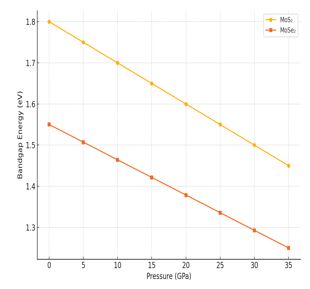
Layered transition metal dichalcogenides (TMDs), particularly molybdenum disulfide (MoS₂) and molybdenum diselenide (MoSe₂), have garnered substantial attention due to their tunable bandgaps, strong excitonic effects, and layered structures. These unique properties render those promising candidates for next-generation optoelectronic and nanoelectronic devices. In this study, we investigate the structural and optoelectronic modulation of high-purity single crystalline MoS₂ and MoSe₂ under externally applied pressure up to 35 GPa using a diamond anvil cell (DAC) setup. Through in-situ synchrotron X-ray diffraction (XRD), Raman spectroscopy, and photoluminescence (PL) measurements, we observe pressure-induced lattice compression, phonon mode shifts, exciton quenching, and bandgap narrowing, without any evidence of structural phase transition up to the studied pressure range. These findings offer insight into pressure-driven band structure engineering and highlight the potential of TMDs for pressure-tunable optoelectronic devices.
Downloads
References
Chhowalla, M., et al. (2013). Nature Chemistry, 5(4), 263–275.
Wang, Q. H., et al. (2012). Nature Nanotechnology, 7(11), 699–712.
Mak, K. F., et al. (2010). Physical Review Letters, 105(13), 136805.
Splendiani, A., et al. (2010). Nano Letters, 10(4), 1271–1275.
Zhang, Y. J., et al. (2014). Nature Nanotechnology, 9(2), 111–115.
Conley, H. J., et al. (2013). Nano Letters, 13(8), 3626–3630.
Nayak, A. P., et al. (2014). Nature Communications, 5, 3731.
Chi, Z. H., et al. (2014). Physical Review Letters, 113(3), 036802.
Livneh, T., & Sterer, E. (2010). Physical Review B, 81(19), 195209.
Bandaru, N., et al. (2012). Journal of Applied Physics, 111(8), 083532.
Bhattacharyya, S., & Singh, A. K. (2012). Physical Review B, 86(7), 075454.
Mao, H. K., et al. (1986). Journal of Geophysical Research, 91(B5), 4673–4676.
Nayak, A. P., et al. (2014). Nature Communications, 5, 3731.
Livneh, T., & Sterer, E. (2010). Physical Review B, 81(19), 195209.
Chi, Z. H., et al. (2014). Physical Review Letters, 113(3), 036802.
Yun, W. S., et al. (2012). Physical Review B, 85(3), 033305.
Kang, J., et al. (2013). Band offsets and heterostructures of two-dimensional semiconductors. Applied Physics Letters, 102(1), 012111.
Published
How to Cite
Issue
Section
License
Copyright (c) 2025 Bhupendra Mor, Kirti Korot

This work is licensed under a Creative Commons Attribution 4.0 International License.
Research Articles in 'Applied Science and Biotechnology Journal for Advanced Research' are Open Access articles published under the Creative Commons CC BY License Creative Commons Attribution 4.0 International License http://creativecommons.org/licenses/by/4.0/. This license allows you to share – copy and redistribute the material in any medium or format. Adapt – remix, transform, and build upon the material for any purpose, even commercially.
